


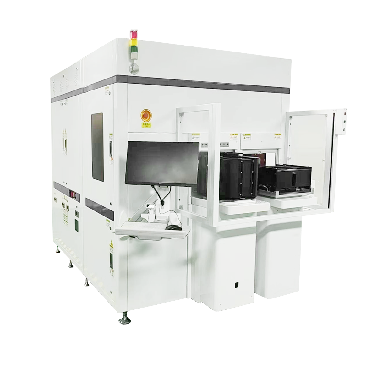
Mainly detect SiC wafer substrate wafers and homogeneous epitaxial wafers: scratches, pits, bumps, stains, microtubules (MP), layer faults (SF), dislocations, etc.


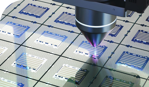
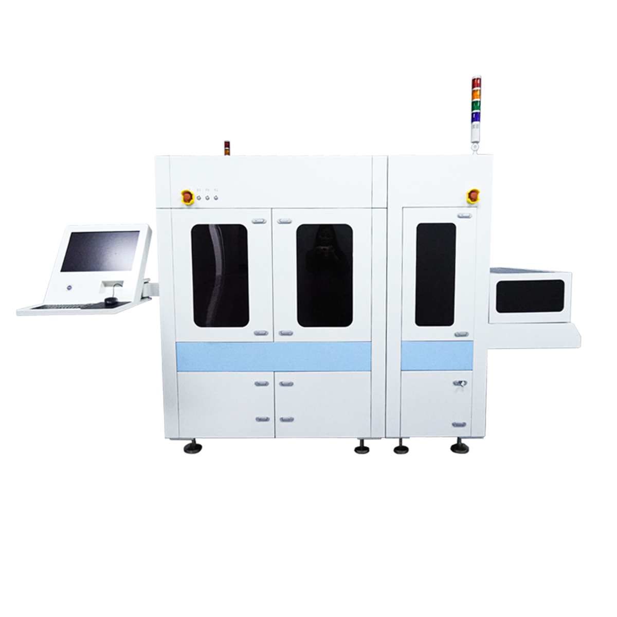
The equipment provides dedicated inspection and metrology solutions for dicing-related processes, with specialized fragmentation detection algorithms to ensure chip integrity
Mainly detect Mico-LED wafer appearance defects: burst, double crystal, scratches, indentation, Sio2 off/ITO off, thin backside plating, missing,
Mainly detect Mini-LED wafer appearance defects: burst point, double crystal, scratches, pressure, Sio2 off/ITO off, back plating thin, chipping edge chipping corner
Inspection items: Mainly detect the TGV microporous hole size, through-hole presence or absence, through the break, cracks, leaks and can not be, foreign matter in the hole, glass slag, dirty


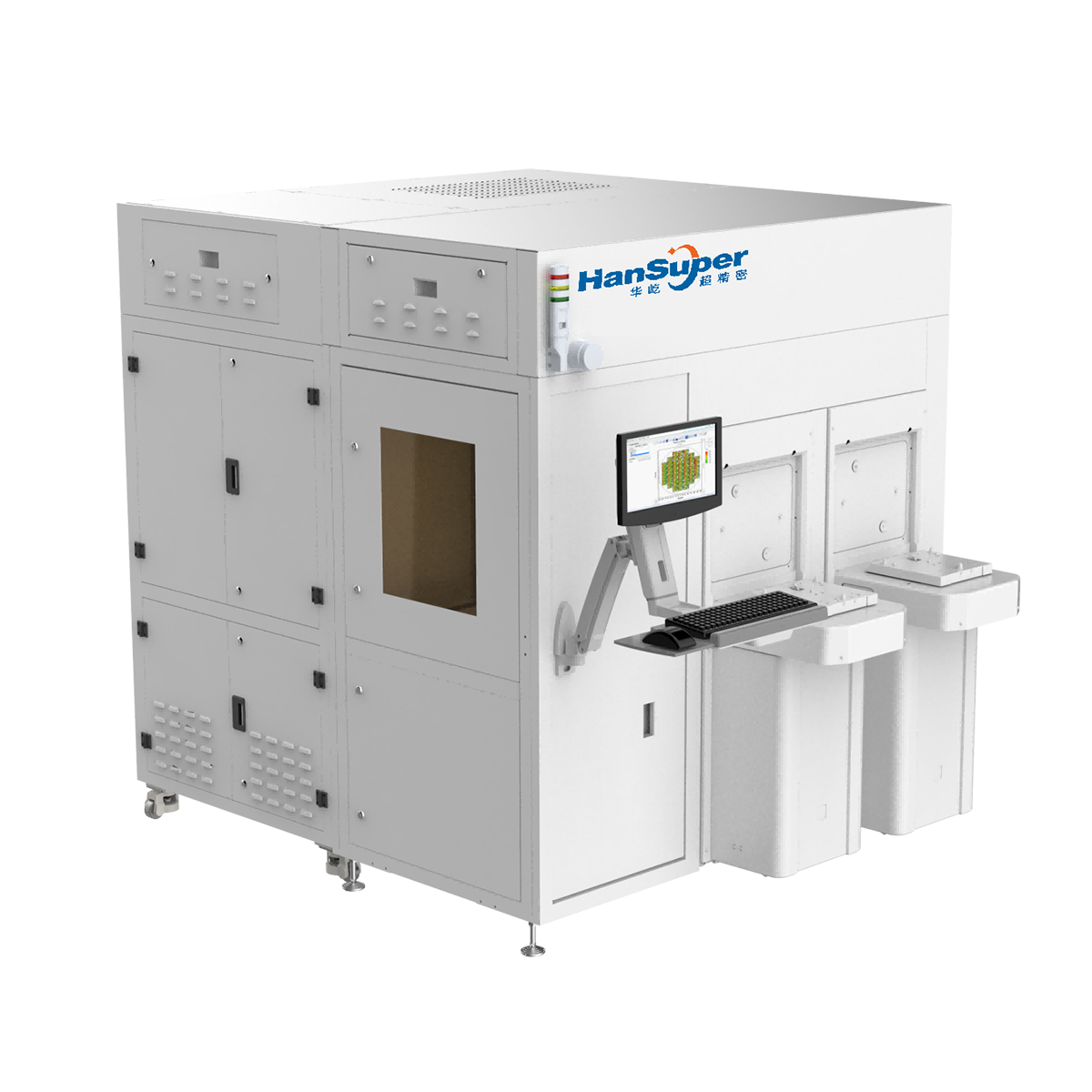
The company has been committed to technological innovation and continuously launches industry-leading equipment products to meet customers' demands for high-quality and high-efficiency equipment.

The company has years of experience in equipment manufacturing and can provide professional customized equipment solutions based on customers' specific needs, meeting their personalized needs and helping them achieve production goals.

The company strictly controls product quality, adhering to high standards and strict requirements in every aspect from raw material procurement to production and manufacturing, ensuring that customer technical requirements are met and equipment can operat

The company has established a comprehensive after-sales service system, including equipment installation and commissioning, technical training, regular maintenance, and a fast response fault handling mechanism, allowing customers to have no worries during