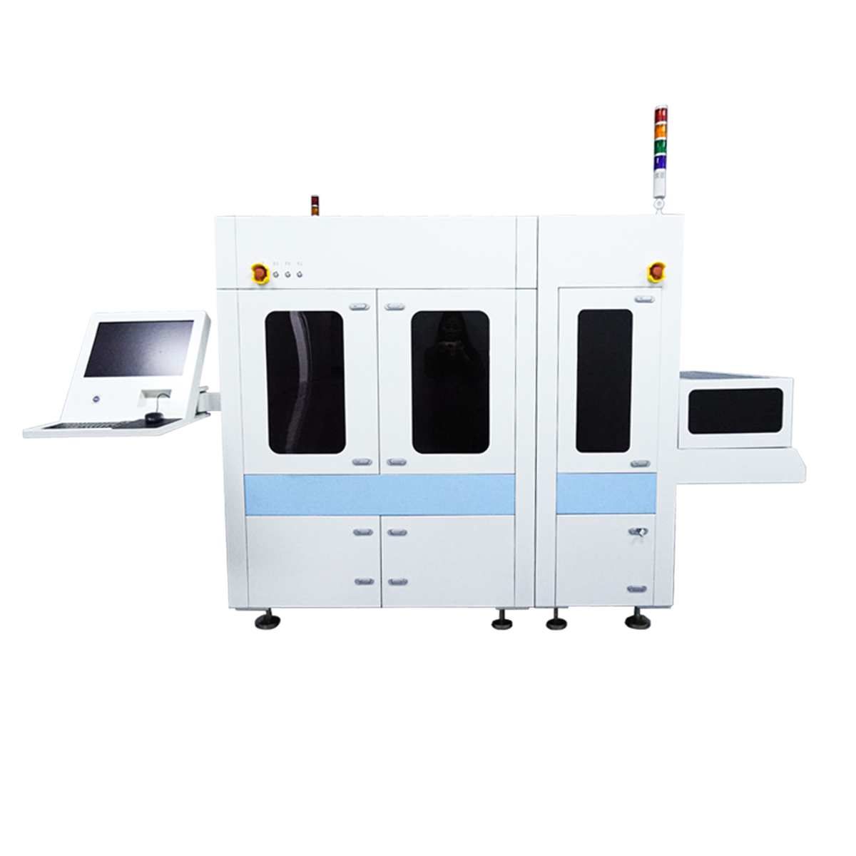
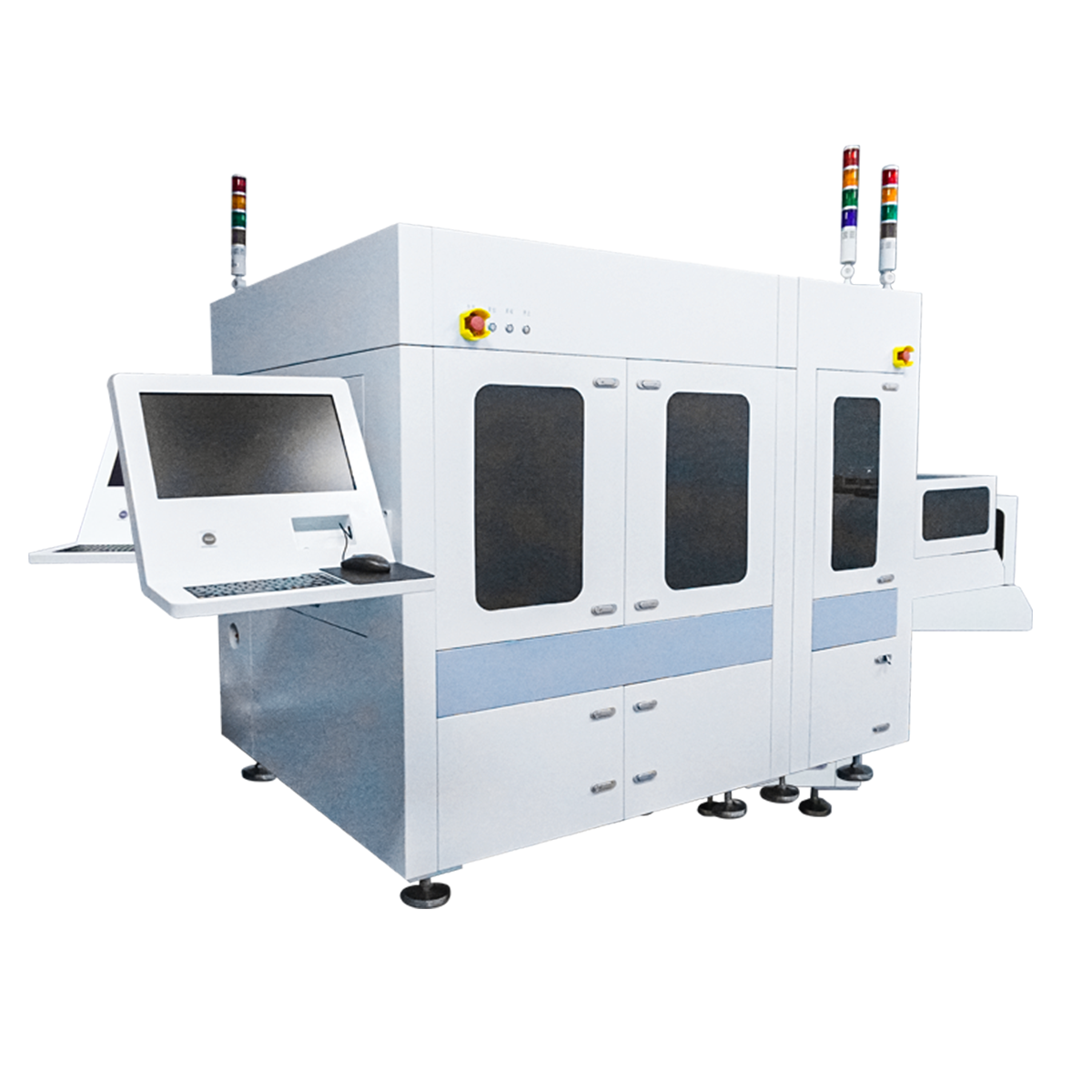
Product Introduction
For the detection of defects in the appearance of Micro LED wafers, we design a special microscopic optical inspection system and defect intelligent detection AI classification algorithm, combined with a high-precision and high-speed marble mobile platform, to intelligently determine various types of defects and extract and classify them, which can effectively solve the pain points of quality control of MicroLED wafers in the manufacturing process.
Product Features
1.Support 4‘ / 6’ / 8’ wafer detection, minimum detection chip size 1mil * 1mil;
2. micro-optical system to support 2X/5X/10X/20X magnification automatic selection, bright field detection, dark field detection imaging;
3. Mainly detect burst point, double crystal, scratches, pressure wound, Sio2 off/ITO off, back plating thin, missing, Finger defects (broken, missing, bent, scratched), small green light, DBR, electrode contamination, RIE, electrode missing, chipping edge chipping corner, light-emitting area contamination, multi-gold, light-emitting area defects, black spots, cut bias, no needle marks and other defects;
4. Based on self-developed AI defect automatic detection and classification algorithms, output defect categories, coordinates, dimensions, and generate defect Map (support TSK, TE).


 Home
Home

 Testing items