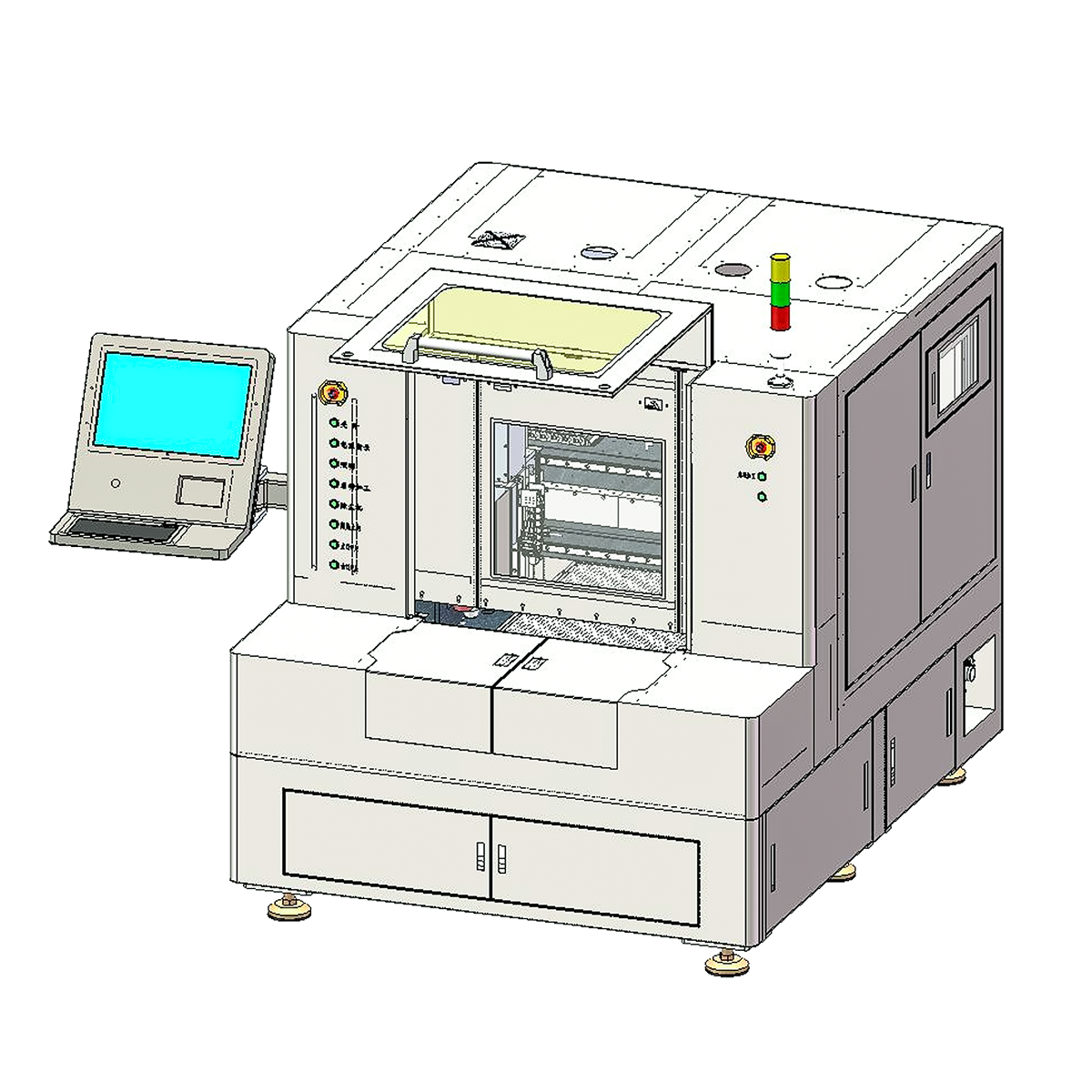
Product Introduction
For the IGBT industry ceramic substrate in the production process of how to identify defective defects in the detection needs, through the design of a dedicated optical inspection system and defect intelligent detection AI classification algorithms, combined with high precision and high speed of the marble mobile platform, intelligent determination of various types of defects, and extracted and classified, an effective solution to the IGBT ceramic substrate production process of the pain point of quality control.
Product Features
1. Detection speed 0.25sec/FOV, 2D detection resolution up to 10um/Pixel;
2.Mainly detect the surface of ceramic substrate scratches, indentation, oxidation, wrinkled skin, foreign objects, chipping, short circuit, open circuit and other defects at any location;
3. Compatible fixture size range: 510mm * 460mm, support customization;
4. Modular optical path sealing design, high stability optical path transmission structure;
5. Excellent loss of graphic reading and processing capabilities, instantaneous processing of oversized graphics;


 Home
Home


 Testing items